Localization of Japanese Patterns
□ Schematic drawing
□ Symbols and footprint
□ Mainstream EDA softwares
□ Date conversion and optimization
□ High-speed interface design
□ HDI buildup and blind vias
□ Standard structure and Card


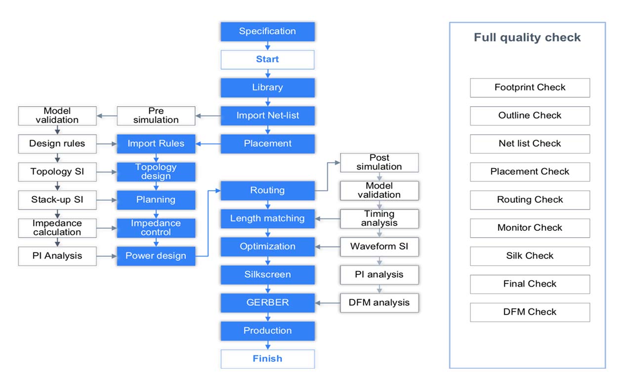
PCB Design


Cooperate ( technical and training) with senior Japanese design company, complete with Japanese-style management and process.
Well-built design methods, strict double check, effective deadline management, details orientated.
To Japan for technical training, to master the most advanced technical information, give full consideration to EMI, EMC and design for manufacturability.
10+ years of design experience design with manufacturing feasibility track and optimize from design until manufacturing.
High frequency, high speed and high density, digital and analog, large power and large current, software and hard ware combination.
□ Schematic drawing
□ Symbols and footprint
□ Mainstream EDA softwares
□ Date conversion and optimization
□ High-speed interface design
□ HDI buildup and blind vias
□ Standard structure and Card
46
+
Layers
36000
+
Connections
58000
+
Pins
1521
+
BGA Pins
64
+
BGA Count 1 Board
36
mil -
Width and Spacing
4.4
GHz +
Frequency
30
Gbps +
Rate

Main board/High-speed backplane, Graphics/Network card, Optical module, Switch...

Mobile phone, Pad, Set-top boxes, Digital cameras, Smart wearables...

Medical equipment, Automation, Machinery, Security, ATE, Testing...

ECU, TCU, BCM, NEV, Autonomous, Information...

Rail transit, Navigation, Aviation, Aerospace, Carrier vehicles...